

Designing for Low Power
Battery life in an embedded product is rarely decided by the datasheet parameters. It is decided much earlier, by architecture choices that compound silently through the entire program — and are painful to unwind once the schematic is frozen. This article collects what has proven out across several low-power data-logger and wearable programs, with a bias toward the decisions that matter most and the ones that most often go wrong.
The target audience is the engineer standing at the start of a new low-power program: choosing an MCU, sketching a firmware architecture, arguing with mechanical about battery volume. If a single-charge runtime of days or weeks is on the requirements list, the decisions in the first few weeks will set the ceiling for what any later optimization can recover.
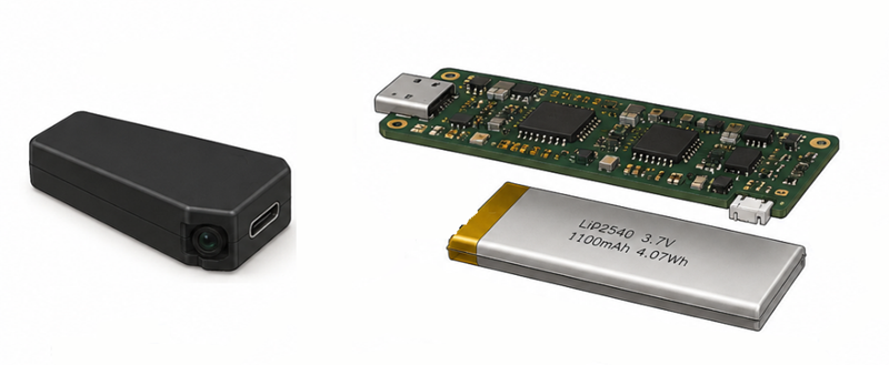 Figure 1: Small Lithium-Ion Battery used in small wearable device
Start With the Power Budget, Not the Datasheet
The first real deliverable of a low-power program is a power budget derived from the use case, not from vendor sleep-mode current numbers. The use case dictates how often the system wakes, how long each wake lasts, which peripherals are active during that wake, and how long the system sits idle between wakes. The product of these numbers, not the MCU's advertised sleep current, determines battery life.
A typical mistake is to anchor the budget on the MCU's deep-sleep current and assume the rest of the system will follow. In practice, the MCU is often one of the lower contributors to quiescent draw. A sensor with an internal voltage reference that cannot be powered down, a communication transceiver with an always-on clock, a fuel-gauge IC with a 5 µA housekeeping current, and the leakage through the power-gating transistors themselves will routinely sum to more than the MCU's own sleep current. Budget every net, not just the ones vendors advertise.
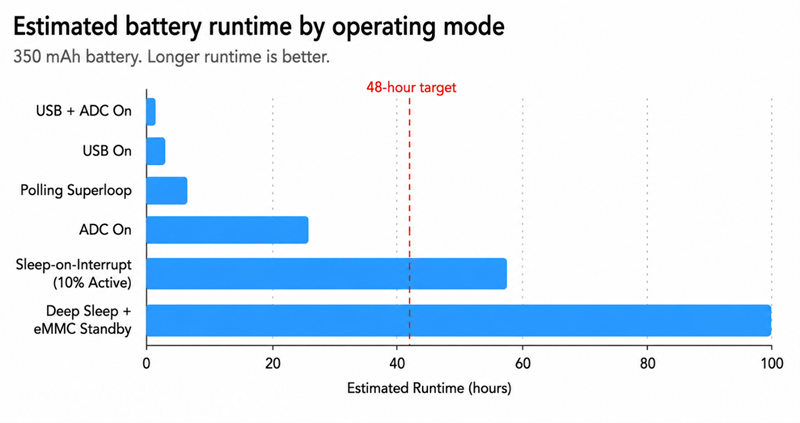 Figure 2: Runtime impact by peripheral operation
On a recent wearable sensor program targeting 40–48 hours of runtime from a 350 mAh cell, the polled-scheduler architecture turned out to be the single largest constraint on closing the power budget. Every optimization that followed — sensor timing, clock tree, eMMC clock rate — had a ceiling imposed by how often the main loop was busy-waiting on I²C transactions rather than opportunistically entering WFI (Wait For Interrupt, the Cortex-M instruction that halts the CPU clock until the next interrupt). That constraint was baked in two years before anyone measured it.
|
The MCU's advertised sleep current sets the floor for what is achievable. Everything else in the system sets the ceiling for what you actually get. |
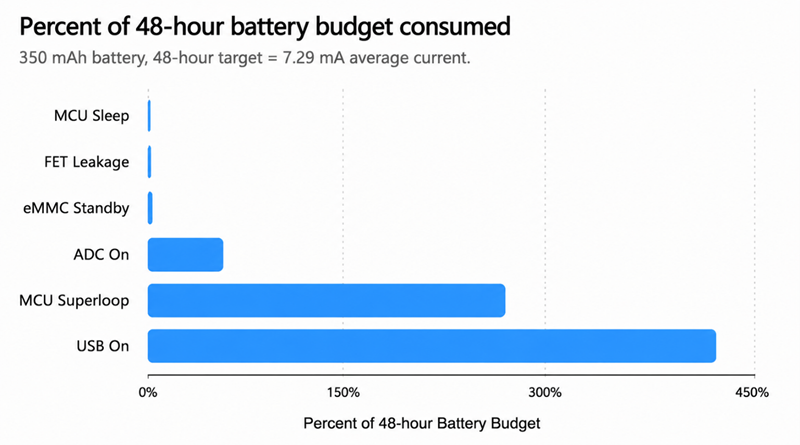
Figure 3: USB and firmware architecture consume multiple times the entire battery budget
MCU Selection: Peripherals You Don't Use Still Cost You
MCU selection for low-power applications goes beyond the sleep-mode current listed on the front page of the datasheet. The practical questions are: Which clocks must remain active in each sleep mode? How quickly can the device wake up? How granular is peripheral clock gating? And which peripherals can be fully power-gated rather than merely clock-gated?
A peripheral that is only clock-gated (peripheral clock is disabled but is still powered) still dissipates leakage current through its own gate oxide, port protection diodes, and level shifters. A peripheral that has been power-gated (its power domain disabled) draws effectively zero power. The difference between these two states can be tens of microamps per peripheral on a modern MCU, and an MCU with, say, eight unused peripherals that can only be clock-gated will quietly bleed several hundred microamps that never appear in a back-of-envelope estimate.
The distinction is subtler than "off means off." A peripheral can be asleep (clock stopped, registers retained) without being disabled. A peripheral can be disabled (logic inactive) without being powered down. And a peripheral can be powered down (rail disabled) while its analog or communication front end (AFE or PHY) is still drawing current from a separate always-on domain. USB is a common example.
Disabling the controller does not automatically disable the transceiver, which can consume milliamps on its own. Another example is the ADC. Disabling the converter does not necessarily power down the internal voltage reference, the input buffer, or the bias network that feeds them. Datasheets usually include a block-level power diagram. For a low-power design, the entries that matter are which blocks are shut down by which control bits and the current consumption of each block.
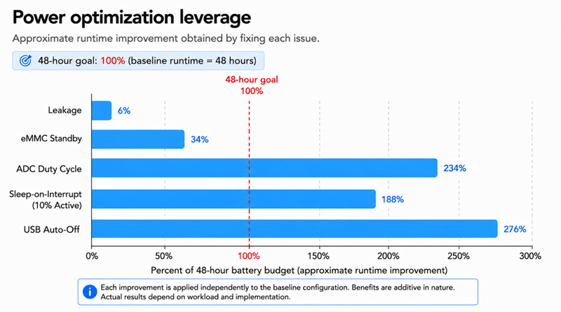 Figure 4: Opportunities to improve/optimize power consumption
Practical selection criteria that have proven out:
- Multiple independent low-power modes, not just a single "sleep" state. The flexibility to trade wake-up latency against quiescent current is essential.
- DMA on every peripheral that moves bulk data. DMA operates independently of the CPU, shuffling bytes between a peripheral and memory without executing instructions, which means the CPU can be in a low-power state during the entire transfer and only woken up by the DMA completion interrupt to process data. When the DMA is not used the CPU must wake up to manually move bytes from an SPI receive buffer, using more power than if the DMA was used.
- A real-time clock on its own power island, with its own low-frequency oscillator, not sharing a domain with anything else.
- The ability to retain a small region of SRAM across deep sleep, so waking from sleep does not require reinitializing the entire application state.
- A wake-up latency that is a small fraction of the wake-up duty cycle. Waking up is not free, as the MCU burns through microjoules of energy while the PLL locks and the flash controller warms up, and that energy is charged to every wake event.
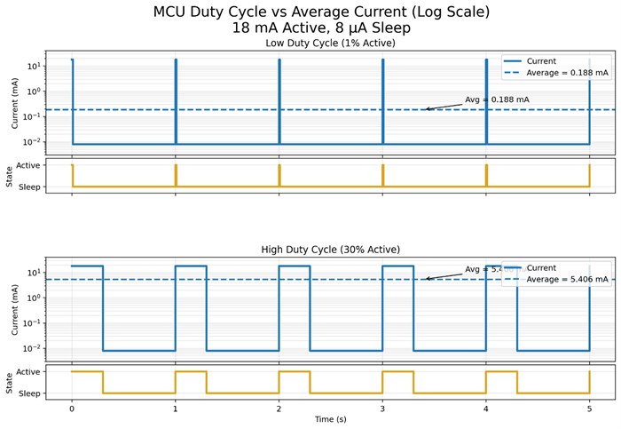 Figure 5 Reducing MCU on-time by sleeping between events/tasks reduces overall power consumption
On MCUs such as the ATSAMS70 family, which I have been developing with recently, the peripheral ID mapping in the PCER0 and PCER1 registers is worth reviewing carefully before beginning any optimization work. Every peripheral whose clock is not explicitly gated off in your initialization sequence is drawing current at MCK rate, regardless of whether your firmware ever touches it. Default reset state is not the same as the state that minimizes current, and the difference on a fully populated MCU can exceed a milliamp.
Availability Is Now Part of the Selection
The technical criteria above are necessary but not sufficient. An MCU that meets every requirement on paper but has a 52-week lead time, or is on allocation, or has a question mark next to its long-term supply status, is not a viable selection regardless of how good the datasheet looks. The chip-supply experience of the last several years has made this a first-class selection criterion rather than a footnote.
The practical question to answer before committing is: when is the product actually going to production, and what will availability look like at that moment? A part chosen today because it is in stock today may be unobtainable in six months when the prototypes turn into a purchase order. Conversely, a part that is nominally in catalog may be de facto unavailable in quantity, with every broker listing it at a 10× markup and with an 8-week lead time. Distributor stock, manufacturer lifecycle status, multi-source availability, and the existence of pin-compatible alternates are all part of the selection now, and none of them have anything to do with the datasheet.
The defensive move is to choose an MCU family with multiple pin-compatible devices, ideally from a vendor with a stable roadmap and a history of long production lifetimes. A firmware port to a compatible device is a two-week effort; a firmware port to an entirely different MCU architecture could take a year. Component volatility is now a design input.
Firmware Architecture: Where the Real Savings Live
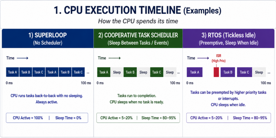
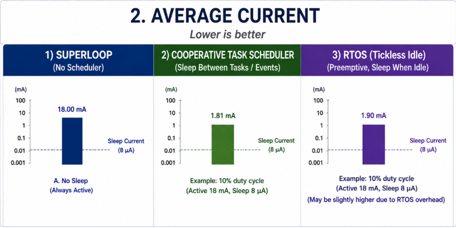
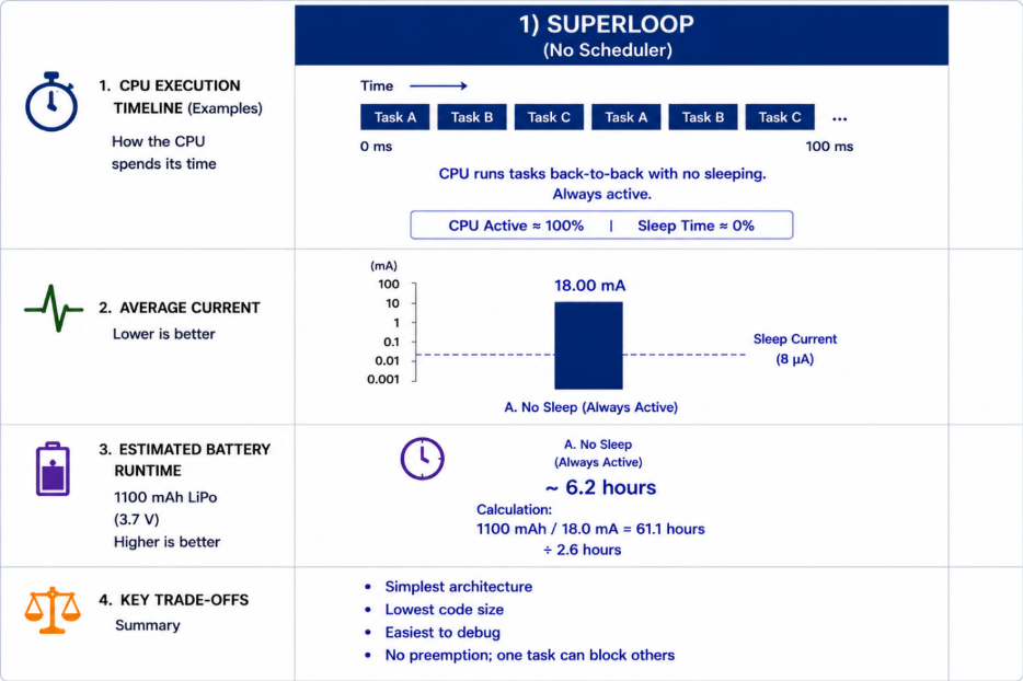
Three firmware architectures used for low-power embedded products are the superloop, the cooperative task scheduler, and the RTOS. Each has a natural low-power ceiling, and that ceiling is usually the binding constraint on battery life once the hardware is fixed.
The Superloop
A single while(1) {} loop that polls and dispatches. Simple to write, easy to debug, and entirely adequate for a product whose activity is dominated by a periodic wake followed by a short burst of work followed by a long sleep. The low-power ceiling for a superloop is high if the loop structure explicitly yields to a sleep call at the bottom of every pass. If the loop is constantly polling a flag, a register, or an I²C completion, the MCU is running at full clock rate with the only payoff being that you can see where you are in the loop with a debugger.
The Cooperative Scheduler
A small homebrew scheduler that dispatches tasks from a timer tick. Better organized than a superloop, easier to profile tasks, and it lends itself to clean low-power patterns. Each task runs to completion, returns, and if no other task is ready, the scheduler drops into WFI until the next tick. The risk is that polled I/O inside a task breaks this pattern as thoroughly as it breaks a superloop. A cooperative scheduler is only as low-power as its most-polling task.
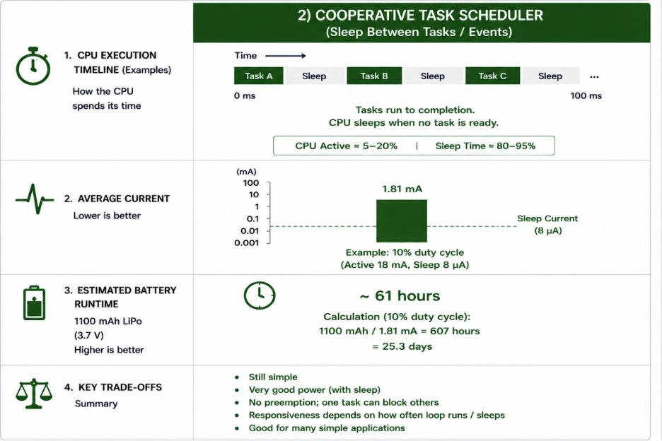
The RTOS
A preemptive RTOS, correctly configured for tickless idle, is the architecture most naturally suited to deep low-power operation. Tasks block on semaphore, queue, timeout events and the idle task hands control to the kernel's low-power hook, which determines the next scheduled wake-up, configuring the sleep mode accordingly. The kernel does the accounting that a superloop programmer would have to do by hand.
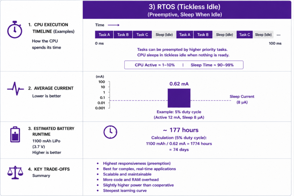
The cost of the RTOS is real: driver development is harder, debug tooling is heavier, and there is a learning curve for the team. But for any product where the runtime target is measured in days, and where multiple asynchronous events need to be handled without polling, the RTOS earns its keep. Zephyr and FreeRTOS are the two we have recently used with good results; both support tickless idle with mature device driver models for power management.
The trap I've personally experienced on several programs is that the architecture is chosen in the first two weeks of the program, based on familiarity or schedule, and the power implications are not revisited until the first power measurement six months later. By that point, converting a polled superloop to an event-driven RTOS is a three-month rewrite that the schedule cannot absorb. Make the architecture decision with the power budget in hand, not beside it.
Power Gating: FET vs BJT
Disabling functional sections and power supplies when they are not needed is the single largest lever for reducing average current. The transistor choice for the power-gate switch itself is less obvious than it appears.
MOSFETs are the default. They offer very low RDS(on) when fully enabled — down to tens of milliohms for a typical SOT-23 small-signal device, and single-digit milliohms for power packages — so they can handle the full load current without dissipating significant heat. They switch fast, they need almost no steady-state gate current, and the logic level threshold variants interface directly with MCU GPIO without any level shifting.
BJTs, despite being less fashionable, have one consistent advantage in low-power designs: their leakage current when fully off is typically an order of magnitude lower than a MOSFET of comparable capability. For a power gate that spends 99% of its life in the off state, such as a sensor rail, a communication module, a peripheral power domain, the quiescent leakage through the switch is what dominates the off-state current, and a BJT can cut that by 10× or more.
A well thought out design might take advantage of both: MOSFETs for rails that see high peak current when enabled, and BJTs for rails that are disabled most of the time and whose total on-time energy is small. The decision comes down to a simple accounting: the energy lost to RDS(on) × I² × ton versus the energy lost to Ileak × V × toff. For short duty cycles, leakage wins. For long duty cycles or high peak currents, conduction wins.
Battery Monitoring: Good Enough vs Sophisticated
Two techniques dominate battery state monitoring, and the right one depends on the precision the product needs and the quiescent current it can afford to spend.
Voltage-Threshold Sleep
The simplest approach: characterize the battery's discharge curve at the load profile the product will see, determine a voltage below which continued operation risks under-voltage damage, and sleep the system when that threshold is crossed. This requires only a voltage divider into an ADC channel, costs a few microamps when active (and zero when the ADC is off), and is entirely adequate for a product that does not need to report state-of-charge to the user with any precision.
The characterization effort is real. The discharge curve of a lithium cell varies with load current, temperature, and aging, and a threshold that is safe for a fresh cell at room temperature may be insufficient for the same cell at 0 °C after 200 cycles. The voltage at which the pack protection IC triggers under-voltage lockout is the hard floor; the firmware threshold should sit comfortably above it with margin for the pack to rest and recover between measurements.
Coulomb Counting
A dedicated fuel-gauge IC integrates the charge flowing into and out of the pack, with temperature and aging compensation, and is calibrated with the cell's empirical resistance tables. The result is a state-of-charge estimate that is accurate to a few percent across the full discharge curve, and that degrades gracefully as the cell ages.
The costs are a continuous quiescent current from the fuel gauge itself, possibly 1 – 10 uA when idling and 20 – 100 uA when actively measuring, and a development investment in characterizing the cell so the gauge's resistance and capacity tables match the actual cell behavior. For a product whose runtime target is single-digit days, the 10 µA is a non-trivial fraction of the total budget, and the threshold-sleep approach may be preferable. For a product whose runtime target is weeks to months and whose user interface requires a meaningful battery percentage, the coulomb counter earns its place.
A fuel gauge running with default cell model tables will report numbers, but those numbers will drift from reality in ways that are difficult to diagnose after the fact. Proper characterization requires several charge/discharge cycles at defined temperatures and load profiles. These results are stored in the gauge to provide an accurate model.
The Compounding Lesson
The architecture decisions covered here — power budgeting from the use case down, MCU selection with peripheral power-down granularity in mind, firmware architecture chosen with the power target in hand, thoughtful use of FETs and BJTs as power gates, and an honest appraisal of how much battery monitoring precision the product actually needs — compound multiplicatively. None of them alone will hit a demanding runtime target. All of them together, chosen consistently in the first weeks of a program, will.
The programs where battery life fell short of the target were not programs where any single decision was catastrophically wrong. They were programs where each individual decision was defensible in isolation but none of them were optimized for low power as a system. The remedy is not heroic late-stage optimization; it is getting the early decisions right, with the power budget visible on every design review slide, from day one.
